![]()


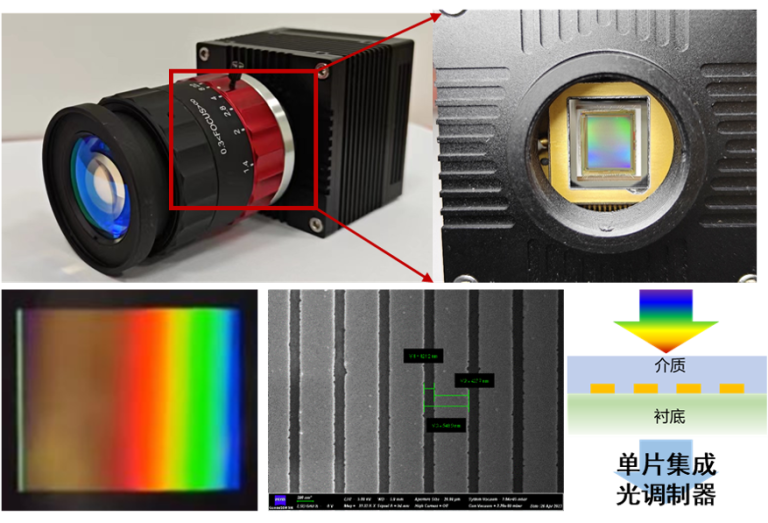
Development of Multifunctional Infrared Chips and Industrial Application of Imaging Systems
Focusing on the development of China's new generation artificial intelligence, this project is aimed at the development of multifunctional infrared chips and the industrial application of imaging systems. The key focus is on the research and development of core components for monolithic hybrid integrated multifunctional infrared imaging systems, specifically the on-chip integration of metasurface-based optical modulators, multifunctional infrared chips. The project will utilize micro-nano metasurfaces to achieve multiple photon property regulation, including wavelength filtering, polarization control, and phase modulation, in order to build a customized multifunctional infrared imaging system.
Monitoring Large-Amplitude Motion Postures through Light and Shadow Interaction
Shadows are parts of objects that are obscured in a light field. Photodetectors can monitor changes in human body shadows in real time, enabling the recognition of large-scale human movements and postures. At the same time, photodetectors that respond to different wavelengths can precisely identify multi-dimensional human motion shadows. The project aims to reconstruct large-scale human motion postures from the perspective of light and shadow interaction, and, in conjunction with virtual reality technology, to achieve accurate projection from real motion postures to virtual motion postures. Additionally, the project will focus on designing and developing highly engaging, portable, and precise gaming equipment.
Research on Medium and Short-Wave Infrared Imaging of Colloidal Quantum Dots and its Focal Plane Detector Module
Aiming at the civilian market in the field of infrared optoelectronic imaging, which currently lacks affordable detectors, we employ liquid-phase synthesis of infrared colloidal quantum dots with high yield and low cost. This approach overcomes the need for molecular beam epitaxy required by conventional bulk materials such as InGaAs and HgCdTe. By combining precision temperature control and spectral purification, the size uniformity of quantum dots is ensured. Additionally, the difficulty in scaling up arrays caused by flip-chip bonding is resolved, enabling medium and short-wave infrared imaging on a megapixel-scale focal plane array. Through the development of multi-specification colloidal quantum dot infrared detectors with customizable cut-off wavelengths in the range of 1.5-5.0 µm, we significantly reduce the cost of chip modules, addressing current industry cost challenges. This research will lead to the development of integrated and low-cost infrared detection components for outdoor night vision, assisted driving, and industrial sorting. It will also drive technological advancements in wide-spectrum imaging, gas detection, and semiconductor detection.
Investigation on Single-Molecule Fluorescence Microscopic Imaging and Cancer Cell Visualization Devices
Focusing on “Healthy China 2030 initiative” and the comprehensive strategy of cancer prevention and management, this project aims to utilize single-molecule fluorescence imaging and tracking technology combined with microfluidic approach for high-throughput detection to develop a portable, multimodal, ultra-high-resolution molecular imaging diagnostic device. This device will enable real-time quantitative detection of key factors in common tumor cells. By developing highly stable, photoswitchable, and highly sensitive fluorescent probes, we propose in this project to label specific biomarkers within tumor cells, and to excavate precise and personalized molecular diagnostic kits for detection of tumor cells in early stages. A specific, integrated, and digitized single-molecule fluorescence microscopy imaging system will be established and promoted in clinical diagnostic platforms, disease control centers and some other applicable venues.
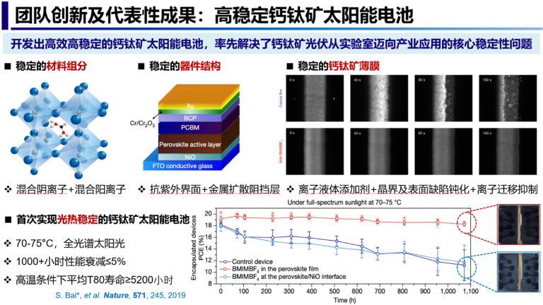
Large-Area Semi-Transparent Perovskite Solar Technology
Facing the future development of high-efficient and stable silicon-perovskite tandem solar cell technology, this project focuses on the research and development of large-area, highly stable and semi-transparent perovskite solar cell modules. Based on the low-cost solution processing techniques, the project aims to develop efficient continuous deposition processes for large-area, high-quality perovskite films, improving key reliability indicators such as environmental stability, photothermal stability, and electric field stability of perovskite films. The project also optimizes the plans of the functional layers and device interfaces in semi-transparent perovskite solar cells and conducts device aging tests for market application, establishing related reliability evaluation standards. This initiative aims to capture the early strategic advantages in the industrialization of perovskite solar cell technology, promoting the commercial development of silicon-perovskite tandem photovoltaic technology, and supporting China in achieving low-carbon transformation and the strategic goals of “carbon neutrality” and “carbon peaking”.
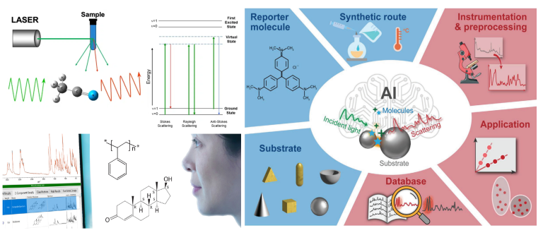
AI-driven Biometrics Using Raman Spectroscopy
By utilizing Surface-Enhanced Raman Spectroscopy (SERS) for high-throughput, non-destructive imaging, the unique optical and physical properties of noble metal nanomaterials, and the advanced feature recognition capabilities of artificial intelligence, this project aims to develop a Big Model for biometric recognition using Raman spectroscopy, and an integrated portable device to inspecting the biomarker related to common ailment in a high-throughput, real-time and quantitative way. Different from the classical pipeline in SERS development, which included identification, optimization, discovery, and evaluation, we are building a specific, integrated, digital, and interpretable Raman detection system and device through the following steps: AI-driven design of substrate enhancement, molecular construction for Raman signal, optimization on synthesis pathway, improvement on experiment instrument, and establishment of data processing and analysis pipeline. This system and device will be further applied in hospitals, centers of disease control, customs, and other inspection areas.
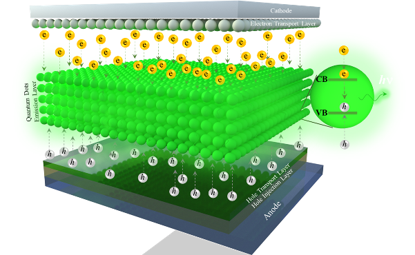
Research on Eco-Friendly Quantum Dot Light-Emitting Diodes and Integrated Display Technology
Targeting next-generation wide color gamut, high-resolution and eco-friendly display technology, this project focuses on the development of eco-friendly semiconductor colloidal quantum dots with low-cost, high quantum yield, tunable and ultra-narrow emission characteristics. The goal is to achieve cost-effective, energy-efficient, environment-friendly, and wide color gamut RGB quantum dot light-emitting diodes (QLEDs). This includes developing quantum dot patterning and QLED device encapsulation technology, overcoming challenges related to efficient electrically-driven QLED chip integration process, meeting the requirements for future high pixel density, high brightness, full-color, ultra-high definition and large-size display technology, and expanding the industry market for near-eye display applications such as virtual/augmented reality displays.
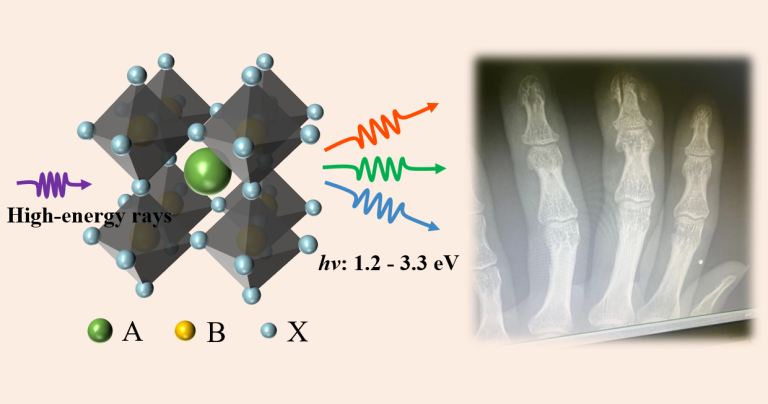
Research on High-Performance Scintillators and X-Ray Detectors
In response to the urgent need for high-performance scintillator materials in fields such as dynamic imaging in modern nuclear medicine, treatment of special diseases and tumors, anti-terrorism security checks, and space polar exploration, this project focuses on the development of scintillator materials, such as perovskite materials, organometallic complexes, and rare earth nanoparticles, with low detection limits, high resolution, and stable performance in extreme environments. The project will also explore matching application technologies for novel scintillation crystals with commercially available optoelectronic detectors like CMOS and TFT, and design special micro-nano optical structures or scintillator arrays to achieve high-resolution X-ray detectors. Additionally, the construction of core-shell structures or functionalizing the surface of scintillation crystals will enhance the radiation stability of materials, and the targeted movement of nanoparticles will facilitate in vitro imaging of lesions and tumors, targeted drug release and treatment of specific diseases.
Research on Intelligent High-Energy Photon Nuclear Medicine
Focusing on the innovative development of nuclear medical technology, this study utilizes high-energy photon petal accelerators to explore the stability, adjustability, thermal sensitivity, and targeting of α/β-type radioactive nuclides. The main objectives include the development of multimodal imaging, therapeutic monitoring functions, and precise disease state identification using radioactive pharmaceuticals. The goal is to create a comprehensive drug information database based on nuclides, drug molecules, and target information, breaking the boundaries of traditional medicine. By integrating technological innovation with practical clinical application needs, this research will facilitate the translation of high-energy photon nuclear medical technology into real-world applications.
Development and Industrialization of On-Chip Optofluidic Lab Devices
This project focuses on the development, system integration, and application of fully optical lab-on-a-chip (LOC) devices. Key areas of research include the integration of optofluidic control components such as pumps, valves, flow meters, and detection units. The project aims to establish multifunctional integration on optofluidic chips for processes like transport, storage, mixing, and separation, minimizing the need for external devices. Applications in environmental monitoring, disease diagnosis, drug screening, and biochemical research are prioritized. The key development involves intelligent medical instruments, single-molecule detection chips, and optofluidic chips for cell sorting and culture. The goal is to enable fully optical-controlled chemical reactions, nucleic acid amplification, and protein analysis within the chip.
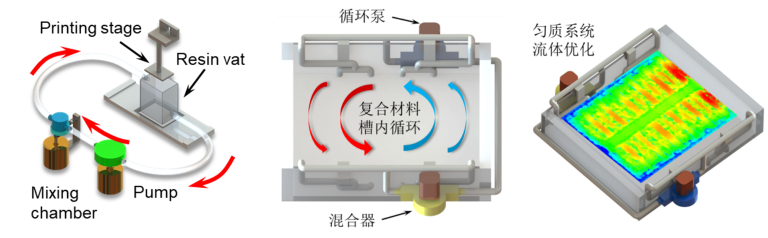
Advanced Additive Manufacturing of Microwave and Optical Metamaterial and Micro-Nano Devices
As the functionality of microwave and optical devices for 5G communication, optical computing chips, and quantum communication chips improves, their structural complexity drastically increases. Existing manufacturing processes can no longer meet the demands of such microwave and optical micro-nano devices. Additive manufacturing, with its high design freedom, offers a new method of producing micro-nano devices with complex structures. This project addresses the key scientific and technical challenges in the integration of structure and function for the manufacturing of microwave and optical micro-nano devices by leveraging the circulating vat photopolymerization technology developed by the research team for high-quality composite materials additive manufacturing. The research aims to develop a full-chain process, covering materials, equipment, and design and devices, with a strong focus on the materials property tuning, forming mechanisms, microstructure control, and structural design of microwave and optical metamaterials-based micro-nano devices based on additive manufacturing. The project aims to develop composite materials, such as ceramics or ceramic precursors, specifically for additive manufacturing of microwave and optical metamaterial micro-nano devices, optimize device manufacturing processes, demonstrate applications and eventually realize technology translation.
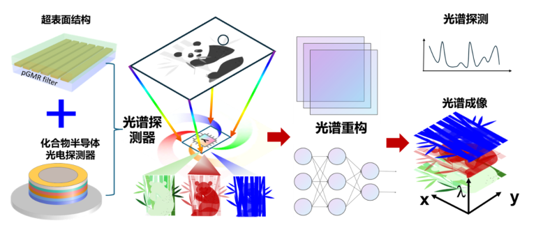
High-Performance Infrared Spectroscopy Detection and Imaging System Research
Focusing on the strategic development of intelligent detection equipment, this project aims to address the critical shortcomings in China's intelligent detection equipment industry, including key electronic components. By integrating infrared spectroscopy detection and imaging technology with optical field modulation techniques using micro-nanostructures, semiconductor device carrier transport modulation techniques, and efficient spectral reconstruction technology, this project seeks to overcome the challenges of traditional spectroscopic detection systems, such as large volume, complex structure, high cost, insufficient spectral resolution, and low detection efficiency. The goal is to develop wide-spectrum, high-spectral-precision, high-efficiency, low-cost infrared spectroscopy detectors and imaging systems. Building on infrared spectroscopy detection and imaging technology, the project will develop highly integrated gas detection systems and multifunctional material screening intelligent detection equipment, supporting the construction of informationization and intelligentization in China.

Research on intelligent medical image analysis and diagnosis system based on digital twin and quantum image
Focusing on the “Healthy China 2030” strategy and the development needs of precision medicine, this project aims to integrate medical image data of different modalities using multimodal fusion technology, and to improve the comprehensiveness of diagnostic information and the detection of small lesions by combining quantum imaging processing technology for image segmentation and enhancement. Through digital twin technology, the project will create a digital pathological process model of patients. Coupling this with deep learning technology, an intelligent diagnostic model will be built, enabling real-time data monitoring, dynamic simulation, and automatic detection. The goal is to establish an integrated, informative, and personalized medical image analysis and diagnostic system, promoting its application in clinical diagnosis platforms, disease control centers, and other markets.
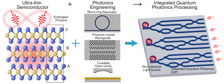
Integrated chip hosting compact nonclassical photon sources
Semiconductor light sources are critical to the advancement of modern electronics and the semiconductor industry. Building on Chengdu's thriving semiconductor ecosystem, this project aims to develop an integrated photonic chip that hosts an innovative non-classical photon source for next-generation information technologies. Currently, existing non-classical photon source products typically rely on bulk nonlinear crystals. In contrast, this project will deliver a highly compact photon source—at the micrometer scale—and capable of generating non-classical light such as entangled photons and squeezed light. The project will combine mature semiconductor fabrication techniques with a novel ultra-thin semiconductor material, two-dimensional 3R-MoS₂, and parametric nonlinear down-conversion technology. 3R-MoS₂ is exceptional not only for its ultra-strong optical nonlinear effects, which enable the creation of more compact non-classical light sources compared to other materials, but also for its promising physical properties, such as ferroelectricity, opening up potential applications in non-volatile memory. Its two-dimensional structure further facilitates hybrid integration into other integrated photonic devices, providing a significant advantage over existing products. By replacing bulky light sources with a compact chip, this project provides a critical technological component that will enable a wide range of applications, from photonic and quantum computing to secure communications and intelligent sensing.
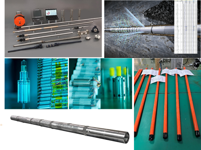
Localization and Industrialization of Key Oil and Gas Drilling Equipment Based on Multi-Dimensional Wireless Sensing
This project focuses on key technologies for oil and gas extraction, aligning with national energy development priorities. It aims to break the monopoly of Western countries on China's oil drilling and extraction equipment. Centered on oil and gas drilling technology, the project develops core components of multi-dimensional wireless sensing devices, including multi-dimensional sensors, key detection chips, high-temperature battery modules, and wireless sensing systems. These innovations ensure safe and efficient energy extraction in complex and harsh environments characterized by moisture, high temperatures, and turbulence. The project aims to provide diverse, systematic, and stable multi-dimensional wireless sensing solutions for China's oil and gas drilling industry. By promoting technological innovation and localization in oil and gas extraction, it contributes to the country's energy independence and self-sufficiency.
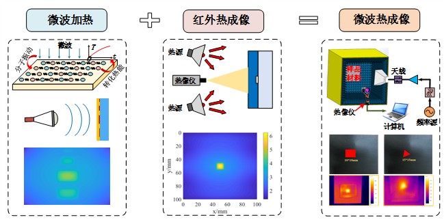
Research on Microwave Thermal Imaging-Based Detection Technology for Debonding of Radar-Absorbing Coatings
This project focuses on the non-destructive detection of debonding defects in radar-absorbing coatings during both indoor and outdoor maintenance. Leveraging the high microwave absorption characteristics of radar-absorbing coatings, it integrates microwave heating with infrared non-destructive testing and proposes a microwave thermal imaging-based debonding detection technique. Compared with traditional infrared non-destructive testing, microwave thermal imaging requires lower power and is easier to integrate into systems. Additionally, by utilizing the penetration capability of microwaves in coating materials, this method enhances the interaction between microwaves and coatings, thereby improving defect detection performance in infrared thermal imaging. Ultimately, this project aims to provide theoretical and technical support for on-site inspection of radar-absorbing coatings and enrich the field inspection system for coating materials.
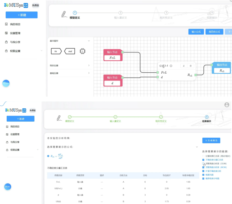
Measurement Uncertainty Statistical Analysis Software
Focusing on the needs for scientific and standardized uncertainty analysis in the field of testing and measurement, this solution adheres to international standard ISO/IEC GUIDE 98-3:2008, national standard GB/T 27418-2017, and metrology regulations JJF 1059.1/2-2012. It supports both the GUM method and the Monte Carlo Method (MCM) for simultaneous computation. Built-in mathematical and statistical analysis methods cover all aspects of experimental evaluation, including statistical analysis of test data, modeling of measurement systems (or processes), analysis of uncertainty sources, Monte Carlo analysis, direct uncertainty evaluation of physical parameters, and uncertainty evaluation of complex derived parameters. It can be used to analyze and report measurement uncertainty, assess and control measurement systems or processes, and manage measurement decision risks. The platform allows rapid setup of uncertainty analysis systems tailored to different testing environments. With a four-step fast calculation process, intelligent formula parsing, and zero programming required, it fills the gap in China for general-purpose measurement uncertainty statistical analysis software.
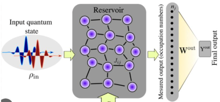
Exploiting quantum dynamics for machine learning applications
Quantum many-body systems and their rich dynamical features have huge potential for computational tasks. By leveraging the principles of quantum mechanics, such as superposition, entanglement, and coherence, quantum dynamics can enhance the efficiency and accuracy of machine learning tasks. In this project we mainly focus on two signal processing tasks: (i) image processing and; (ii) time series analysis. In the former, by incorporating the information of an image into the Hamiltonian of a many-body system, one can exploit the discriminative behavior of many-body dynamics for image classification. In the latter, the inherent temporal evolution of quantum systems can be harnessed to model complex temporal dependencies, improving predictions of time series, such as financial data, weather forecasting, and biomedical signals. In these projects, we integrate quantum many-body physics with classical machine learning frameworks, to achieve greater precision in both image processing and time series analysis.
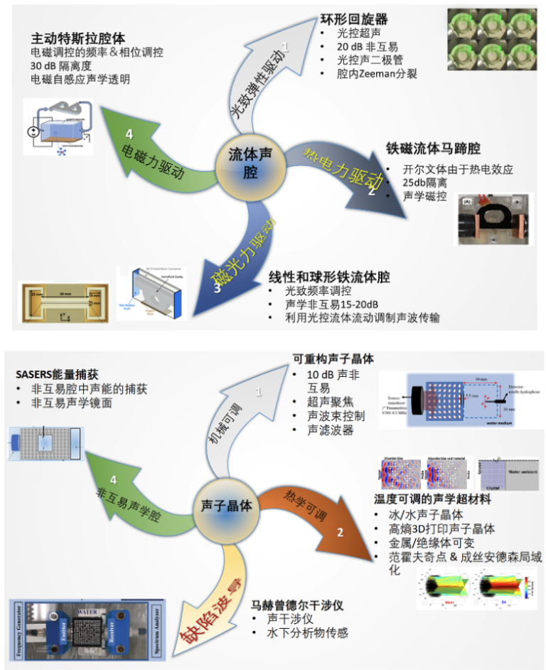
China Acousto Photonics Translational Alliance (CAPTA) Light-inspired macromachines and phononic technologies offer the opportunity to develop a new class of aquatic devices based on optoelectronic principles
Emerging optically driven and photonic enhanced ultrasound platforms can fuse Professor Arup Neogi’s recent breakthroughs in tunable phononic‐crystal acoustics with China’s mature photonics and manufacturing infrastructure to create a new generation of versatile “acousto photonic” devices. Four core technologies underpin this translation pathway. (i) Laser cavitation induced acoustic filters, diodes, and modulators using acoustic cavities and metamaterials. (ii) Thermally and optically tunable phononic crystal meta lenses—fabricated from stimulus-responsive hydrogels and actuated by 1.55 µm laser micro heaters—yield sub-wavelength (λ/4) focusing at clinically relevant depths (3 MHz, >10 cm), enabling handheld super-resolution ultrasound probes. Use these metalens to develop novel ultrasonic elastography-based diagnostic techniques for biomedical imaging, such as bone-tissue differentiation and deep tissue imaging. (iii) Use acoustic metalens and elastography for in-situ diagnostics of additive manufacturing. Estimate the mechanical properties of 3D printed structures. iv. We also propose to realize a new class of underwater machines and acoustic devices that can be used for underwater communication using well-established photonic technology. A phased translation program (TRL 4 prototypes in 2026; TRL 6 pilots by 2028; TRL 8 certified products by 2033) combines academic strengths at UESTC, SJTU and West China Hospital with industrial partners.